- 您现在的位置:买卖IC网 > Sheet目录1990 > CDP68HC68T1M (Intersil)IC RTC 32X8 NVSRAM CMOS 20-SOIC
4
FN1547.8
October 29, 2007
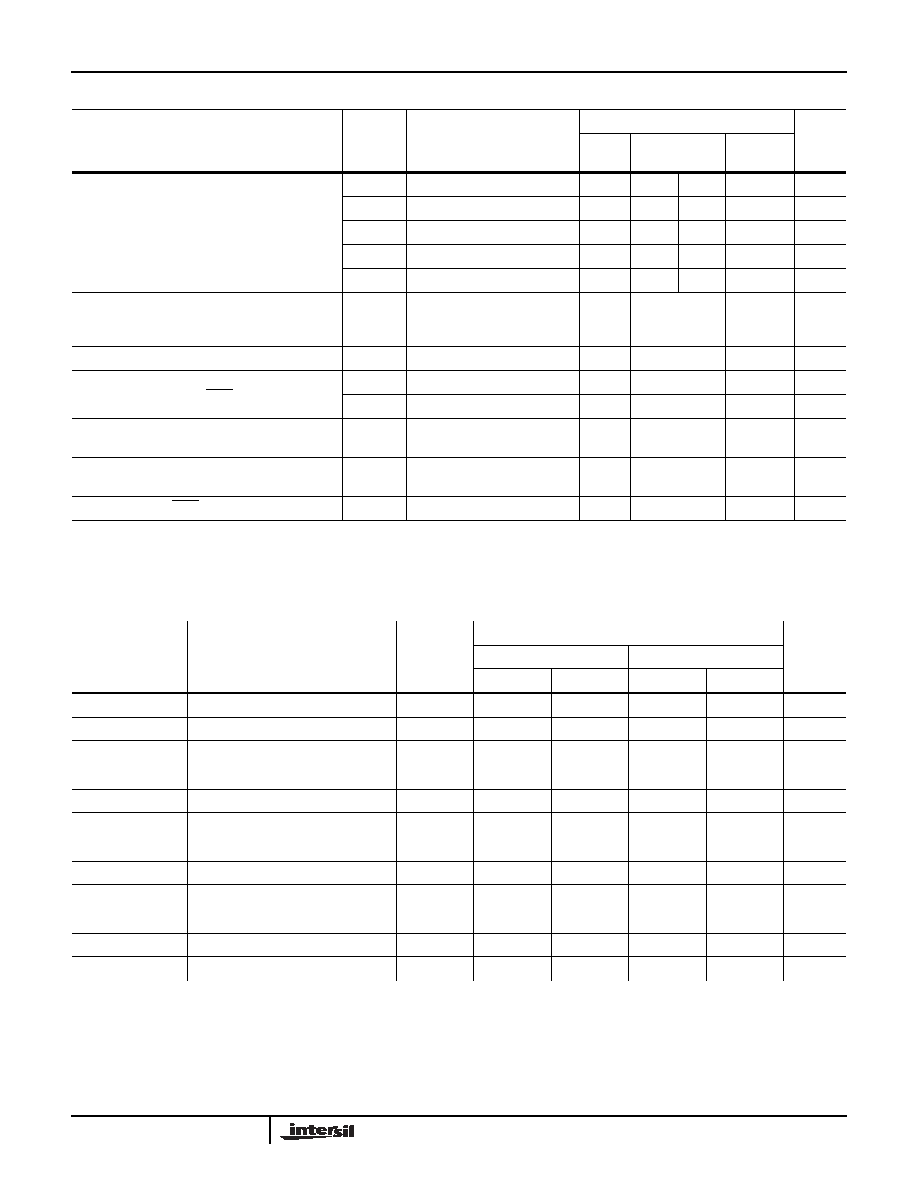
Operating Current (Note 3)
VDD = 5V, VB = 3V
Crystal Operation
ID
IB
-mA
32kHz
-
0.025
0.015
-
mA
1MHz
-
0.08
0.15
-
mA
2MHz
-
0.15
0.25
-
mA
4MHz
-
0.3
0.4
-
mA
Standby Current (Note 3)
VB = 2.2V
Crystal Operation
IB
32kHz
-
10
-
A
Input Capacitance
CIN
VIN = 0, TA = +25°C
-
2
pF
Maximum Rise and Fall Times
(Except XTAL Input and POR Pin 10)
tr, tf
--
2
s
--
s
Input Voltage (Line Input Pin Only, Power Sense
Mode)
010
12
V
VSYS > VBVT
(For VB Not Internally Connected to VDD)
-1.0
-
V
Power-On Reset (POR) Pulse Width
100
75
-
ns
NOTES:
2. Typical values are for TA = +25°C and nominal VDD.
3. Clock out (Pin 1) disabled, outputs open circuited. No serial access cycles.
Dynamic Electrical Specifications
Bus Timing VDD ±10%, VSS = 0VDC, TA = -40°C to +85°C
IDENTIFICATION
NUMBER
PARAMETER
SYMBOL
LIMITS (ALL TYPES)
UNITS
VDD = 3.3V
VDD = 5V
MIN
MAX
MIN
MAX
1
Chip Enable Setup Time
tEVCV
200
-
100
-
ns
2
Chip Enable After Clock Hold Time
tCVEX
250
-
125
-
ns
3
Clock Width High
tWH
400
-
200
-
ns
4
Clock Width Low
tWL
400
-
200
-
ns
5
Data In to Clock Setup Time
tDVCV
200
-
100
-
ns
7
Clock to Data Propagation Delay
tCVDV
-
200
-
100
ns
8
Chip Disable to Output High Z
tEXQZ
-
200
-
100
ns
11
Output Rise Time
tr
-
200
-
100
ns
12
Output Fall Time
tf
-
200
-
100
ns
A
Data in After Clock Hold Time
tCVDX
200
-
100
-
ns
B
Clock to Data Out Active
tCVQX
-
200
-
100
ns
C
Clock Recovery Time
tREC
200
-
200
-
ns
Static Electrical Specifications At TA = -40°C to +85°C, VDD = VBATT = 5V ±5%, Unless Otherwise Specified. (Continued)
PARAMETER
SYMBOL
TEST CONDITIONS
CDP68HC68T1
UNITS
MIN
TYP
(Note 2)
MAX
CDP68HC68T1
发布紧急采购,3分钟左右您将得到回复。
相关PDF资料
CPLL66-1600-2200
IC VCO PLL/SYNTH 2.2GHZ SMD
CPLL66-2175-2175
IC VCO PLL/SYNTH 2175MHZ SMD
CPLL66-2400-2500
IC VCO PLL/SYNTH 2500MHZ SMD
CPLL66-2450-2450
IC VCO PLL/SYNTH 2450MHZ SMD
CPLL66-3160-3380
IC VCO PLL/SYNTH 3380MHZ SMD
CPLL66-3475-3475
IC VCO PLL/SYNTH 3475MHZ SMD
CPLL66-4160-4380
IC VCO PLL/SYNTH 4380MHZ SMD
CPLL66-4240-4240
IC VCO PLL/SYNTH 4240MHZ SMD
相关代理商/技术参数
CDP68HC68T1M2
功能描述:实时时钟 PERIPH SPIAL-TIME- CLK 16W IND RoHS:否 制造商:Microchip Technology 功能:Clock, Calendar. Alarm RTC 总线接口:I2C 日期格式:DW:DM:M:Y 时间格式:HH:MM:SS RTC 存储容量:64 B 电源电压-最大:5.5 V 电源电压-最小:1.8 V 最大工作温度:+ 85 C 最小工作温度: 安装风格:Through Hole 封装 / 箱体:PDIP-8 封装:Tube
CDP68HC68T1M296
功能描述:实时时钟 PERIPH SPIAL-TIME- CLK 16W INDEL RoHS:否 制造商:Microchip Technology 功能:Clock, Calendar. Alarm RTC 总线接口:I2C 日期格式:DW:DM:M:Y 时间格式:HH:MM:SS RTC 存储容量:64 B 电源电压-最大:5.5 V 电源电压-最小:1.8 V 最大工作温度:+ 85 C 最小工作温度: 安装风格:Through Hole 封装 / 箱体:PDIP-8 封装:Tube
CDP68HC68T1M296S2357
制造商:Rochester Electronics LLC 功能描述:- Bulk
CDP68HC68T1M2Z
功能描述:实时时钟 PERI SPIAL-TIME-CLK RoHS:否 制造商:Microchip Technology 功能:Clock, Calendar. Alarm RTC 总线接口:I2C 日期格式:DW:DM:M:Y 时间格式:HH:MM:SS RTC 存储容量:64 B 电源电压-最大:5.5 V 电源电压-最小:1.8 V 最大工作温度:+ 85 C 最小工作温度: 安装风格:Through Hole 封装 / 箱体:PDIP-8 封装:Tube
CDP68HC68T1M2Z96
功能描述:实时时钟 PERI SPIAL-TIME-CLK RoHS:否 制造商:Microchip Technology 功能:Clock, Calendar. Alarm RTC 总线接口:I2C 日期格式:DW:DM:M:Y 时间格式:HH:MM:SS RTC 存储容量:64 B 电源电压-最大:5.5 V 电源电压-最小:1.8 V 最大工作温度:+ 85 C 最小工作温度: 安装风格:Through Hole 封装 / 箱体:PDIP-8 封装:Tube
CDP68HC68T1M96
功能描述:实时时钟 PERIPH SPIAL-TIME- CLK 20W INDEL RoHS:否 制造商:Microchip Technology 功能:Clock, Calendar. Alarm RTC 总线接口:I2C 日期格式:DW:DM:M:Y 时间格式:HH:MM:SS RTC 存储容量:64 B 电源电压-最大:5.5 V 电源电压-最小:1.8 V 最大工作温度:+ 85 C 最小工作温度: 安装风格:Through Hole 封装 / 箱体:PDIP-8 封装:Tube
CDP68HC68T1M96S2357
制造商:Rochester Electronics LLC 功能描述:- Bulk
CDP68HC68T1MZ
功能描述:实时时钟 W/ANEAL PERIPH SPIAL -TIME-CLK 20W IND RoHS:否 制造商:Microchip Technology 功能:Clock, Calendar. Alarm RTC 总线接口:I2C 日期格式:DW:DM:M:Y 时间格式:HH:MM:SS RTC 存储容量:64 B 电源电压-最大:5.5 V 电源电压-最小:1.8 V 最大工作温度:+ 85 C 最小工作温度: 安装风格:Through Hole 封装 / 箱体:PDIP-8 封装:Tube